
6-inch InP substrates
Development of larger InP single-crystal substrates is underway. The 6-inch specifications in the manuals support technical discussions and do not indicate current production supply.

PRODUCTS & RESOURCES
Our current focus is 4-inch substrates, alongside 6-inch development. Find product guides, technical specifications and our company profile here.

InP single-crystal substrates are our current primary product. Selection should define size, conductivity type, dopant, surface finish and dislocation grade. Suitability must be validated in the intended epitaxial and device processes.
Dimensions and surface options follow the existing manual. Not every combination is necessarily available; committed specifications and lead times require written confirmation.
Development of larger InP single-crystal substrates is underway. The 6-inch specifications in the manuals support technical discussions and do not indicate current production supply.
Building on our substrate foundation, we intend to extend towards epitaxial wafers. Epitaxial wafers are not presented as an established supply product at this stage.
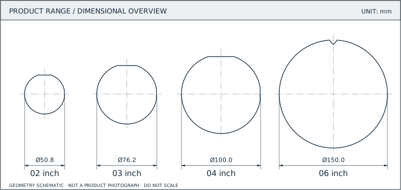
Specification illustration from the existing product documents; not a product photograph or an inventory display.
| Series | Diameter / mm | Thickness / μm | Status |
|---|---|---|---|
| 2″ | 50.8 ± 0.5 | 350 ± 25 | Availability to be confirmed |
| 3″ | 76.2 ± 0.5 | 600 ± 25 | Availability to be confirmed |
| 4″ | 100.0 ± 0.5 | 625 ± 25 | Production capability; configuration to be confirmed |
| 6″ | 150.0 ± 0.5 | 675 ± 25 | In development |
5 documents
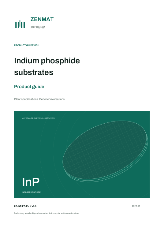
Product selection and technical communication in English.
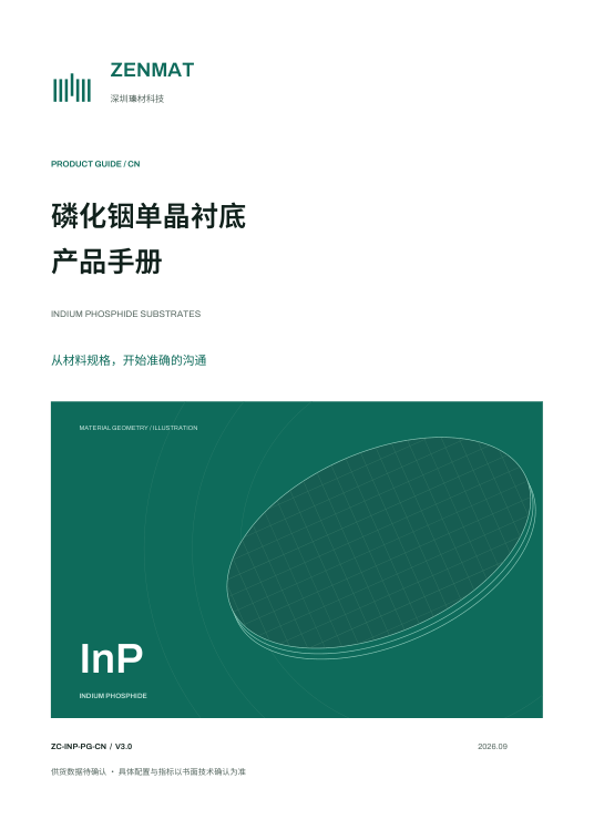
Selection, specifications, quality documents and handling.
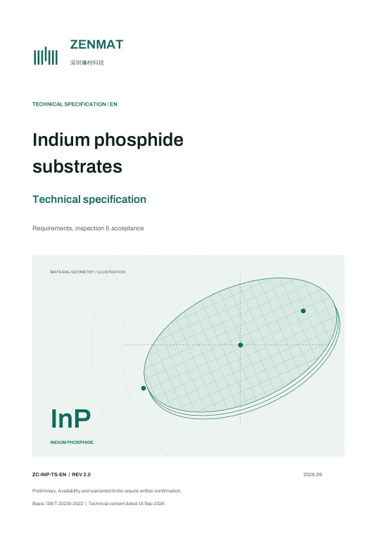
Requirements, inspection and delivery documentation in English.
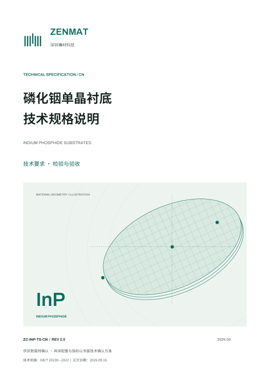
Requirements, drawings, inspection and order confirmation.
Our material focus, approach to specifications and working values.